Pulse Width Modulation
The Pulse Width Modulation wave is used in many application and it essentially acts as a digital signal due to the signal switching from low to high and high to low. The PWM signal is basically an encoded analog signal that is converted into a digital signal for further process. The PWM wave is a square wave with a changing duty cycle based on the analog signal given and it’s frequency is determined based on how fast it finishes a cycle. One application is DC electric motors and the PWM frequency changes as the application change. For example, for the DC electric motors, people usually use a PWM with frequency of 5-10kHz while an Amplifier uses around 20-200KHz.
To generate the PWM, an analog signal and triangle wave is needed, so that both signals feed into a comparator to output the PWM wave. For our project, the analog signal is going to be the audio signal coming from the preamp. Since generating the PWM requires a triangle wave, it is required to generate triangle wave first then move on to the PWM generation. The figure below is the block diagram of the PWM generation.
https://knowledge.ni.com/KnowledgeArticleDetails?id=kA00Z0000019OkFSAU&l=en-US

Figure: PWM generation
The next approach is simulating the triangle wave and understand how it works. It seems that most class D amplifiers uses 555 timers to generate the triangle wave (based on the two schematics that we saw)(backup plan talk about 555astableflipflops). The figure below is the 555 timer circuit connection diagram and the output of the circuit is a triangle wave.


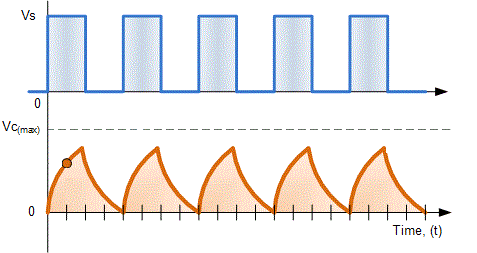
The triangle wave being outputted has voltage of 1.76 peak-peak and frequency of ~233KHz. As you can see from the output, the triangle wave is not a perfect triangle but this will do as fine as a perfect triangle wave. The circuit diagram includes both resistor and capacitor which is forming an RC circuit that is charging the capacitor and discharging it. Because of this, the output is not linear which means both the increase and decrease of the triangle wave is not a straight line. In fact, it is increasing and decreasing exponentially. The charging part of the capacitor is done by feeding the capacitor with certain where as the discharging is being fed with zero voltage and it acts as voltage source which means it is losing voltage over time, this is done by feeding square wave into the capacitor, to visualize that look at the waves below
https://www.electronics-tutorials.ws/rc/rc_3.html (picture reference)
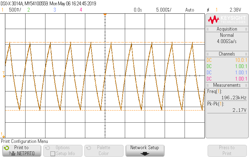
The NE555 timer was used in the simulations due to difficulties implementing the TLC555 in LTSpice. However, the hardware components that will be used is the TLC555. Also, TLC555 uses almost a tenth of the power than the NE555. After wiring and testing the circuit with the TLC555 in the lab, the triangle wave is almost the same as the simulated one but small difference in both frequency and voltage due to the chip changing from NE555 to TLC555. The frequency of the triangle wave is about 200kHz and voltage of 2.17 peak-peak.
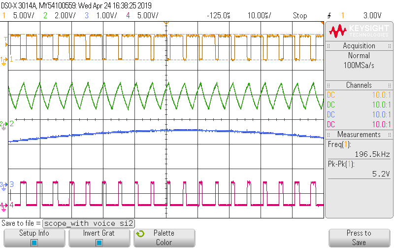
Now the triangle wave generation is done, the comparator takes both the audio signal and the triangle wave as an inputs and outputs the PWM. The IC used as the comparator is LM393 which has two comparators in one IC chip. Based on the datasheet, the comparator is an open collector output which means pull up resistor is needed. An appropriate value for a pull up resistor is 10 times the input impedance which in our case is going to be the input pin of the gate driver. Typically, the pull up resistor value ranges are limited by the range of 1-10k ohms. However, if the input has small leakage current then the pull up resistor value can go up to 1M ohms. The reason why the values of the pull up resistor are limited is because after going above the typical values, the input pin, which is the gate driver input, response to voltage decreases which means slowing the circuit. In our project, the fast response are needed. The reason why the circuit response to voltage decreases is because an RC circuit forms which is the pull up resistor and the capacitance of the wire. Since the gate driver requires PWM and an inverted PWM, one way to get the inverted PWM is to flip the inputs and feed that to the other comparator. The gate driver requires PWM and an inverted PWM to driver the mosfets. The next step was simulating the PWM, below is my circuit connection and the output of the comparator.
http://www.resistorguide.com/pull-up-resistor_pull-down-resistor/
One problem that arises when dealing with the PWM signal is the DC offset that should be implemented on the audio signal. The reason why we have a DC offset is that the audio signal has to be within the range of the triangle wave otherwise the output will not have a duty cycle which is not a PWM signal. The PWM has duty cycle of 100% when the sine wave (which is the audio signal) is at the positive peak and the duty cycle decreases as the sine wave start to decrease, Assuming that the sine wave is almost as same as the triangle wave when it comes to the voltage range. This is also implemented in the lab on a breadboard and the dc offset is different due to the fact that the voltage of the triangle waves of the simulated circuit and hands-on circuit are different. For the oscilloscope screen shots below, the audio signal is 4 KHz , 1.5 Vpp and 1.65 V DC offset.